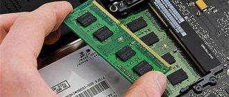
Every computer has RAM, either built into the processor or on a separate board connected to the system—computing devices simply couldn't function without RAM.
RAM is a stunning example of precision engineering, but despite the intricacy of its manufacturing processes, memory is produced in huge volumes every year. It has billions of transistors, but it only consumes a few watts of power. Given the great importance of memory, it is worth writing an intelligent analysis of its anatomy. So, let's get ready for the dissection, roll out the stretcher and go to the anatomical theater. It's time to study all the details of each cell that makes up modern memory and learn how it works.
Why are you, RAM-eo?
Processors need to access data and instructions very quickly so that programs execute instantly.
In addition, they need to ensure that random or unexpected requests do not suffer too much on speed. This is why RAM (RAM, short for random-access memory) is so important for a computer. There are two main types of RAM: static and dynamic, or SRAM and DRAM for short.
We will only consider DRAM because SRAM is only used inside processors such as CPU or GPU. So where is DRAM located in our computers and how does it work? Most people are familiar with RAM because several of its sticks are located next to the CPU (central processing unit, CPU). This group of DRAM is often called system memory, but it is better called CPU memory because it is the main storage of working data and instructions for the processor.
As you can see in the image provided, DRAM is located on small cards that are inserted into the motherboard (system) board. Each board is usually called a DIMM or UDIMM, which stands for dual inline memory module (U stands for unbuffered). We'll explain this in more detail later; for now let's just say that this is the most famous RAM of any computer.
It doesn't have to be super fast, but modern PCs require a lot of memory to run large applications and handle hundreds of processes running in the background.
Another place to find a set of memory chips is usually the graphics card. It requires ultra-fast DRAM because 3D rendering requires a huge number of data reads and writes. This type of DRAM is designed for slightly different uses than the type used in system memory.
Below you can see the GPU surrounded by twelve small platters - these are DRAM chips. This particular type of memory is called GDDR5X, which we will talk about later.
Graphics cards don't require as much memory as CPUs, but they still have thousands of megabytes in capacity.
Not every device in a computer needs so much: for example, hard drives only need a small amount of RAM, on average 256 MB; they are used to group data before writing it to disk.
In these photos we see HDD (left) and SSD (right) boards, with DRAM chips marked on them. Have you noticed that there is only one chip? 256 MB is not such a big amount today, so one piece of silicon is enough.
Once you know that every component or peripheral that does processing requires RAM, you can find memory in the guts of any PC. SATA and PCI Express controllers have small DRAM chips; Network interfaces and sound cards also have them, as do printers and scanners.
If memory is found everywhere, it may seem a little boring, but once you dive into its inner workings, all boredom will disappear!
Conclusion
I hope my information helped you and you were able to find out what RAM and CPU are, because you can see these designations everywhere - now you will know what they mean))
Time to say good-bye. Good luck, health and goodness to you!
There is an opinion among computer users that you can never have too much RAM... And you can’t argue with this, dear reader, especially when it comes to modern machines whose hardware configuration corresponds to solid characteristics, and the Windows system installed on board the PC is 64 -bit version. However, the “painful” problem of many – “the computer’s physical memory is loaded, what should I do” – still continues its inglorious existence, perplexing the average user and sometimes forcing an experienced computer guru to rack his brains over solving the “lack of RAM” problem. However, we will not delve into the extreme complexity of “operational misunderstandings” and will resort to simple, but nevertheless effective methods for diagnosing and optimizing the computer swap system. Well, the article promises to be memorable. RAM secrets are waiting to be revealed!
Scalpel. Clamp Electron microscope.
We don't have all the tools that electronics engineers use to study their semiconductor creations, so we can't just take apart a DRAM chip and show you its innards. However, the guys from TechInsights have such equipment, who took this picture of the chip surface:
If you thought it looked like agricultural fields connected by paths, then you are not so far from the truth! Only instead of corn or wheat, DRAM fields are primarily made up of two electronic components:
- A switch represented by a MOSFET (MOSFET)
- A storage device that is a groove capacitor.
Together they form a so-called memory cell, each of which contains 1 bit of data. A very rough diagram of the cell is shown below (with apologies to electronics experts!):
The blue and green lines indicate the connections that supply voltage to the MOSFET and capacitor.
They are used to read and write data into a cell, and the vertical (bit) line is always fired first. A groove capacitor is essentially used as a vessel to fill with electrical charge - its empty/full state gives us 1 data bit: 0 is empty, 1 is full. Despite the efforts made by engineers, capacitors are not able to store this charge forever and over time it flows away.
This means that each memory cell must be constantly updated 15-30 times per second, although this process itself is quite fast: it takes only a few nanoseconds to update a set of cells. Unfortunately, a DRAM chip has many cells, and while they are being updated, they cannot be read or written to.
Several cells are connected to each line:
Strictly speaking, this diagram is not ideal because there are two bit lines for each column of cells - if we depicted everything, the diagram would become too illegible.
A complete row of memory cells is called a page, and its length depends on the type and configuration of the DRAM. The longer the page, the more bits it contains, but also the more electrical power is needed to operate it; Short pages consume less power but also contain less data.
However, there is another important factor to consider. When reading and writing a DRAM chip, the first step in the process is to activate the entire page. A string of bits (consisting of zeros and ones) is stored in a row buffer, which is essentially a collection of sense amplifiers and latches rather than additional memory. The corresponding column is then activated to retrieve data from this buffer.
If the page is too small, then rows need to be activated more often to keep up with data requests; and vice versa - a large page provides more data, so it can be activated less often. And even though a long string requires more power and can potentially be less stable, it is better to aim for the longest pages possible.
If we put a set of pages together, we get one bank of DRAM memory. As with pages, the size and arrangement of rows and columns of cells play an important role in the amount of data stored, memory speed, power consumption, and so on.
For example, a schema might consist of 4,096 rows and 4,096 columns, with the total capacity of one bank being 16,777,216 bits or 2 megabytes. But not all DRAM chips have square banks because long pages are better than short ones. For example, a design with 16,384 rows and 1,024 columns would give us the same 2 megabytes of memory, but each page would contain four times as much memory as a square design.
All pages in the bank are connected to a row addressing system (the same applies to columns) and they are controlled by control signals and addresses for each row/column. The more rows and columns there are in a bank, the more bits must be used in the address.
A 4,096 x 4,096 bank requires 12 bits for each addressing system, and a 16,384 x 1,024 bank would require 14 bits for row addresses and 10 bits for column addresses. It is worth noting that both systems have a total size of 24 bits.
If a DRAM chip could only provide access to one page at a time, this would not be particularly convenient, so they pack multiple banks of memory cells. Depending on the overall size, the chip may have 4, 8, or even 16 banks—8 banks are most commonly used.
All these banks have common command, address and data buses, which simplifies the structure of the memory system. While one bank is busy working with one team, other banks can continue their operations.
The entire chip, containing all the banks and buses, is packaged in a protective shell and soldered to the board. It contains electrical conductors that supply power for DRAM operation and command, address, and data signals.
The photo above shows a DRAM chip (sometimes called a module) made by Samsung. Other leading manufacturers include Toshiba, Micron, SK Hynix and Nanya. Samsung is the largest manufacturer, with approximately 40% of the global memory market.
Each DRAM manufacturer uses its own system for encoding memory characteristics; The photo shows a 1 gigabit chip containing 8 banks of 128 megabits, arranged in 16,384 rows and 8,192 columns.
Purpose and principle of operation
The main purpose of RAM is to store temporary data that the computer needs only while it is running.
This memory is loaded with data that will be executed by the processor directly.
These include executable files (primarily with the .exe extension) and libraries, the results of various operations that are performed during PC operation, and key press codes such as CapsLock, Ins, etc.
The operating principle of RAM is as follows:
- All memory cells are in their own rows and columns;
- An electrical signal is sent to the selected memory line.
- The signal opens the transistor.
- The charge present in the capacitor is supplied to the desired column connected to a sensitive amplifier;
- The flow of electrons created by the discharged capacitor is detected by the amplifier and leads to the issuance of the corresponding command.
Rice.
2. General scheme of data processing by computer technology. Important : When an electrical signal is applied to a certain line, all its transistors open.
It follows that the minimum amount of data that is read from memory is not a cell, but a row. Due to the fact that RAM is based on semiconductors, the data stored in this memory remains accessible only when an electrical current is applied.
When the voltage is turned off, the power is cut off and all data in the RAM is completely erased.
Higher in rank
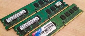
Memory companies take multiple DRAM chips and install them on a single board called a DIMM.
Although the D stands for dual, that doesn't mean it has two sets of chips. By double we mean the number of electrical contacts at the bottom of the board; that is, both sides of the board are used to work with modules. The DIMMs themselves have different sizes and numbers of chips:
The photo above shows a standard desktop DIMM, and below it is the so-called SO-DIMM (small outline, “small profile DIMM”). The small module is designed for small form factor PCs such as laptops and compact desktops. Due to the small space, the number of chips used decreases, the memory speed changes, and so on.
There are three main reasons for using multiple memory chips per DIMM:
- This increases the amount of available storage
- Only one bank can be accessed at any time, so having the others running in the background improves performance.
- The address bus in the processor that processes memory is wider than the DRAM bus.
The latter is very important because most DRAM chips only use an 8-bit data bus.
However, CPUs and GPUs differ from them in this respect: for example, the AMD Ryzen 7 3800X CPU has two built-in 64-bit controllers, and the Radeon RX 5700 XT has eight 32-bit controllers built in. That is, each DIMM that is installed in a Ryzen computer will require eight DRAM modules (8 chips x 8 bits = 64 bits). You might think that the 5700 XT graphics card would have 32 memory chips, but it only has 8. So what does that give us?
Memory chips designed for graphics cards have more banks, usually 16 or 32, because 3D rendering requires simultaneous access to a large amount of data.
One Rank and Two Rank
The set of memory modules that "populate" the data bus of a memory controller is called a rank, and although more than one rank can be connected to a controller, it can only receive data from one rank at a time (because the ranks share the same data bus). This is not a problem because while one rank is busy responding to a command passed to it, another rank can be given a new set of commands.
DIMM cards can have multiple ranks and this is especially useful when you need a huge amount of memory, but there are few RAM slots on the motherboard.
So-called dual- or quad-rank designs can potentially provide greater performance than single-rank designs, but increasing the number of ranks quickly increases the load on the electrical system. Most desktop PCs can only handle one or two ranks per controller. If the system needs more ranks, then it is better to use a buffered DIMM: such boards have an additional chip that eases the load on the system by storing commands and data for several cycles before passing them on.
Many Nanya memory modules and one buffer chip - classic server RAM
But not all ranks are 64 bits in size - DIMMs used in servers and workstations are often 72 bits in size, that is, they have an additional DRAM module. This additional chip does not provide any increase in capacity or performance; it is used for error checking and correcting (ECC).
You remember that all processors need memory to work? With ECC RAM, the small device doing the work is given its own module.
The data bus in such memory is still only 64 bits wide, but the reliability of data storage is significantly increased. The use of buffers and ECC only slightly affects overall performance, but greatly increases the cost.
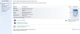
What should you do first if your PC loses performance?
Of course, first of all, you need to diagnose the system. Moreover, everything necessary for this is provided in advance by Microsoft developers. Well, it's time to move on to the practical part of our story.
- Right-click on the taskbar (the lowest area of the screen).
- From the drop-down list, select “Manager...”.
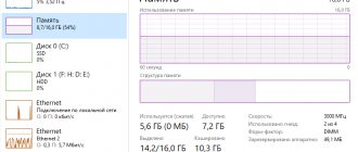
- Once in the work area of the service window of the same name, use the “Performance” tab.
- A visually presented graph will allow you to estimate the RAM utilization rate. If Vista or a later version of Windows OS is installed on your PC, then the value of memory used should not exceed 70-75% of the total nominal value of the physical swap. Otherwise, you need to unload the RAM area.
Need for Speed
All DRAMs have a central input/output clock (I/O, input/output) - a voltage that constantly switches between two levels;
it is used to organize everything running on the chip and memory buses. If we could go back to 1993, we would have been able to purchase SDRAM (synchronous DRAM) memory, which organized all processes by switching the clock signal from low to high state. Since this happens very quickly, such a system provides a very accurate way of timing events. In those days, SDRAM had I/O clocks typically running at 66 to 133 MHz, and one instruction could be sent to DRAM for each clock cycle. In turn, the chip could transmit 8 bits of data in the same period of time.
The rapid development of SDRAM, led by Samsung, led to the creation of a new type in 1998. In it, data transfer was synchronized by the rise and fall of the clock signal voltage, that is, for each clock cycle, data could be transferred twice to DRAM and back.
What was the name of this exciting new technology? Double data rate synchronous dynamic random access memory (synchronous dynamic memory with random access and double data transfer rate). Usually it is simply called DDR-SDRAM or DDR for short.
DDR memory quickly became the standard (which is why the original version of SDRAM was renamed single data rate SDRAM, SDR-DRAM) and remained an integral part of all computer systems for the next 20 years.
The progress of technology has made it possible to improve this memory, thanks to which DDR2 appeared in 2003, DDR3 in 2007, and DDR4 in 2012. Each new version provided improved performance through faster I/O clocks, improved signal systems, and lower power consumption.
DDR2 introduced a change that we still use today: the I/O clock became a separate system that was timed by a separate set of clock signals, making it twice as fast. This is similar to how CPUs use a 100 MHz clock signal to clock, although the internal clock signals are 30-40 times faster.
DDR3 and DDR4 went a step further by quadrupling the I/O clock speed, but in all of these memory types the data bus still used only I/O rise and fall to transmit/receive information (i.e., twice the I/O clock). data transmission frequency).
The memory chips themselves don't operate at huge speeds—in fact, they move quite slowly. The data transfer rate (measured in millions of transfers per second, MT/s) in modern DRAM is so high due to the use of multiple banks on each chip; If there was only one bank per module, everything would be extremely slow.
| DRAM type | Normal chip frequency | I/O clock | Data transmission frequency |
| SDR | 100 MHz | 100 MHz | 100MT/s |
| DDR | 100 MHz | 100 MHz | 200MT/s |
| DDR2 | 200 MHz | 400 MHz | 800MT/s |
| DDR3 | 200 MHz | 800 MHz | 1600 MT/s |
| DDR4 | 400 MHz | 1600 MHz | 3200 MT/s |
Each new version of DRAM is not backward compatible, that is, the DIMMs used for each type have different numbers of electrical pins, connectors and cutouts so that the user cannot insert DDR4 memory into the DDR-SDRAM socket.
From top to bottom: DDR-SDRAM, DDR2, DDR3, DDR4
DRAM for graphics cards was originally called SGRAM (synchronous graphics RAM). This type of RAM has also undergone improvements, and today it is called GDDR for clarity. Now we have reached version 6, and a system with quadruple frequency is used for data transmission, i.e. 4 transmissions occur per clock cycle.
| DRAM type | Regular memory frequency | I/O clock | Data transmission frequency |
| GDDR | 250 MHz | 250 MHz | 500MT/s |
| GDDR2 | 500 MHz | 500 MHz | 1000MT/s |
| GDDR3 | 800 MHz | 1600 MHz | 3200 MT/s |
| GDDR4 | 1000 MHz | 2000 MHz | 4000 MT/s |
| GDDR5 | 1500 MHz | 3000 MHz | 6000 MT/s |
| GDDR5X | 1250 MHz | 2500 MHz | 10000 MT/s |
| GDDR6 | 1750 MHz | 3500 MHz | 14000 MT/s |
In addition to higher transfer rates, graphics DRAM provides additional features to speed up transfers, such as the ability to open two pages of the same bank simultaneously, DDR-running command and address buses, and memory chips with much higher clock speeds.
What's the downside to all these advanced technologies? Cost and heat dissipation.
A single GDDR6 module is about twice the price of an equivalent DDR4 chip, and it gets pretty hot at full speed—which is why graphics cards with lots of super-fast RAM require active cooling to keep the chips from overheating.
Timings and tension
Timing is the duration of the delay in the process of transferring information between various components of computer technology.
Its value directly affects the speed of RAM, and therefore the entire computer (or other device).
Small timing means that operations will be completed faster.
Latency time is inversely proportional to RAM speed.
To solve the problem, RAM manufacturers increase the operating voltage, reducing timings. This allows you to increase the number of operations performed per unit of time, but also requires a more responsible attitude to the choice of memory, which must also match the voltage.
It is also a good option to install the Mem Reduct utility on your PC - a small utility designed to manage and clean up the RAM on your computer. The program can work with unprotected system functions to clear the cache and allows you to select areas to free it.
Bit rate
DRAM performance is typically measured in the number of bits of data transferred per second.
Earlier in this article, we said that DDR4 used as system memory has chips with an 8-bit bus width, that is, each module can transfer up to 8 bits per clock cycle. That is, if the data transfer frequency is 3200 MT/s, then the peak result is 3200 x 8 = 25,600 Mbit per second or a little more than 3 GB/s. Since most DIMMs have 8 chips, you can potentially get 25 GB/s. For GDDR6 with 8 modules, this result would be 440 GB/s!
This value is usually called memory bandwidth; it is an important factor affecting RAM performance. However, this is a theoretical value because all operations within a DRAM chip do not occur simultaneously.
To understand this, let's take a look at the image shown below. This is a very simplified (and unrealistic) representation of what happens when data is requested from memory.
The first step is to activate the DRAM page that contains the required data. To do this, the memory is first told what rank is required, then the corresponding module, and then the specific bank.
The chip is given the location of the data page (the row address) and responds by sending the entire page. All of this takes time and, more importantly, it also takes time to fully activate the row to ensure that the bit row is completely locked before accessing it.
The corresponding column is then determined and a single bit of information is extracted. All types of DRAM transfer data in bursts, packing information into a single block, and a burst in modern memory is almost always 8 bits. That is, even if one bit is retrieved in one clock cycle, this data cannot be transmitted until 7 more bits are received from other banks.
And if the next required bit of data is on another page, then the currently open page must be closed before activating the next one (this process is called pre-charging). All this, of course, takes more time.
All these different periods between the time the command is sent and the required action is performed are called memory timings or delays. The lower the value, the higher the overall performance because we spend less time waiting for operations to complete.
Some of these delays have names familiar to computer fans:
| Timing name | Description | Typical value in DDR4 |
| tRCD | Row-to-Column Delay: number of cycles between activating a row and being able to select a column | 17 cycles |
| C.L. | CAS Latency: number of cycles between addressing a column and starting to transmit a data packet | 15 cycles |
| tRAS | Row Cycle Time: The smallest number of cycles a row must remain active before it can be pre-charging | 35 cycles |
| tRP | Row Precharge time: minimum number of cycles required between activations of different rows | 17 cycles |
There are many other timings and they all need to be carefully tuned so that the DRAM works stably and does not distort data, while having optimal performance. As you can see from the table, the diagram showing the loops in action should be much broader!
Although processes often have to wait while executing, commands can be queued and sent even if the memory is occupied by something else. This is why you see a lot of RAM modules where we need performance (CPU system memory and chips on graphics cards), and much less modules where they are not so important (in hard drives).
Memory timings are configurable - they are not hard-coded in the DRAM itself, because all commands come from the memory controller in the processor that uses this memory. Manufacturers test each chip they make, and those that meet certain speeds at a given set of timings are grouped together and installed in DIMMs. The timings are then stored in a small chip located on the board.
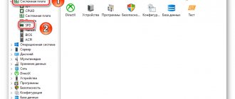
Even memory needs memory.
Red indicates ROM (read-only memory, ROM), which contains SPD information. The process of accessing and using this information is called serial presence detect (SPD). This is an industry standard that allows the motherboard BIOS to know what timings all processes should be set to.
Many motherboards allow users to change these timings themselves either to improve performance or improve platform stability, but many DRAM modules also support Intel's Extreme Memory Profile (XMP) standard. This is just additional information stored in the SPD memory that tells the BIOS: “I can handle these non-standard timings.” Therefore, instead of fiddling with the parameters on their own, the user can configure them with one click.
Types of computer storage devices
Note that there is a permanent memory - these are ROM chips, the transistors of which are capable of being in a certain state in the absence of voltage. Such microcircuits are installed, for example, in hard drives, routers, monitors (saving settings) and other devices where resetting the firmware is not allowed.
Sometimes the term “read-only memory” is used in relation to drives, but this is not entirely correct. You can easily verify this by asking the consultants at an electronics store not for a hard drive, but for a read-only storage device.
There is another modification of data storage solutions, which is a hybrid of RAM and ROM. Thus, the custom BIOS settings of the motherboard are stored in a microcircuit, the transistors of which are supported by an insignificant current received from a rechargeable “coin battery”. This idea has found a “second life” in special drives, the data carriers of which are ordinary memory modules supported by a battery.
Thanks for your service, RAM!
Unlike other anatomy lessons, this one wasn't that messy - DIMMs are difficult to disassemble and require specialized tools to learn the modules.
But there are amazing details hidden inside them. Pick up an 8GB DDR4-SDRAM stick from any new PC: it's packed with nearly 70 billion capacitors and an equal number of transistors. Each one stores a tiny fraction of electrical charge and can be accessed in a matter of nanoseconds.
Even in everyday use, it can execute countless commands, and most of the boards can work for many years without any problems. And all this for less than $30? It's simply mesmerizing.
DRAM continues to improve - DDR5 will appear soon, every module
which promises to achieve levels of bandwidth that are difficult to achieve with two full DDR4 DIMMs. It will be very expensive right out of the box, but for servers and professional workstations this speed jump will be very useful.
See also:
- “Updated SSDs for data centers: large volumes for big guys”
- “External data storage devices: from the time of the IBM 1311 to the present day. Part 1"
- “External data storage devices: from the time of the IBM 1311 to the present day. Part 2"
Another way to free up memory
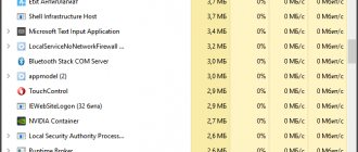
So, in order to see which programs or utilities are “secretly” consuming the kilo- and megabytes of RAM you need so much, do the following:
- Press the key combination “Alt+Ctrl+Del”.
- After you get to the service window that is already familiar to you, open the “Processes” tab.
- Analyze the list presented and use manual correction to turn off the background application that you do not need at the moment.
However, you should not rush to deactivate “aggressive items”, since disabling some critical Windows services can have a detrimental effect on the overall stability of your OS.